
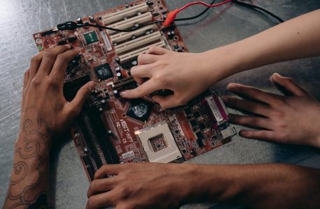
Identifying components on circuit boards involves recognizing parts like resistors, capacitors, and ICs, using visual inspection, datasheets, and tools. This process ensures proper PCB functionality and quality.
What is Component Identification?
Component identification is the process of recognizing and categorizing electronic parts on a circuit board. It involves visually inspecting or using tools to determine the type, function, and specifications of components like resistors, capacitors, and ICs. This step is crucial for troubleshooting, repairs, and ensuring proper PCB functionality. Identification often relies on datasheets, reference designators, and visual cues such as color codes or package shapes. Advanced methods include automated tools and AI-powered systems for faster and more accurate recognition. Accurate component identification ensures that components are used correctly, preventing malfunctions and improving overall circuit performance. It is a foundational skill in electronics engineering and PCB analysis.
Why is Component Identification Important?
Component identification is crucial for ensuring proper PCB functionality, safety, and reliability. It helps in diagnosing faults, performing repairs, and optimizing circuit performance. Accurate identification prevents mismatches, reducing the risk of malfunctions or safety hazards. It also aids in compliance with design standards and simplifies the assembly process. For manufacturers, it ensures traceability and quality control, while for engineers, it supports efficient troubleshooting and design improvements. Proper identification is key to maintaining the integrity and longevity of electronic systems, making it an essential step in both production and maintenance workflows. This process safeguards against errors, ensuring that components meet their intended specifications and roles within the circuit.
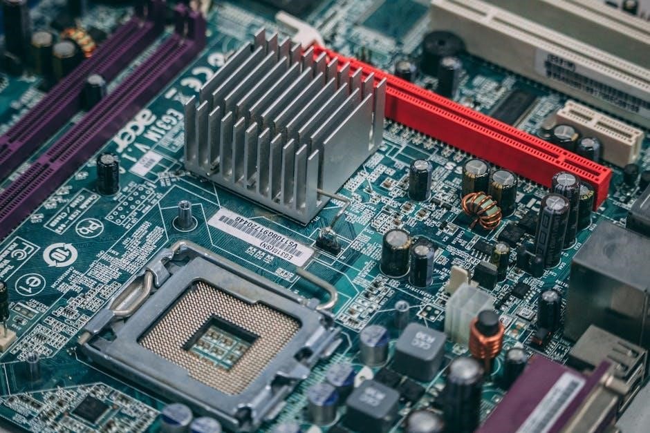
Understanding the Circuit Board
A printed circuit board (PCB) comprises layers, including a solder mask, copper circuits, and substrate, designed to connect components securely, protect circuits, and ensure functionality.
Structure of a Printed Circuit Board (PCB)
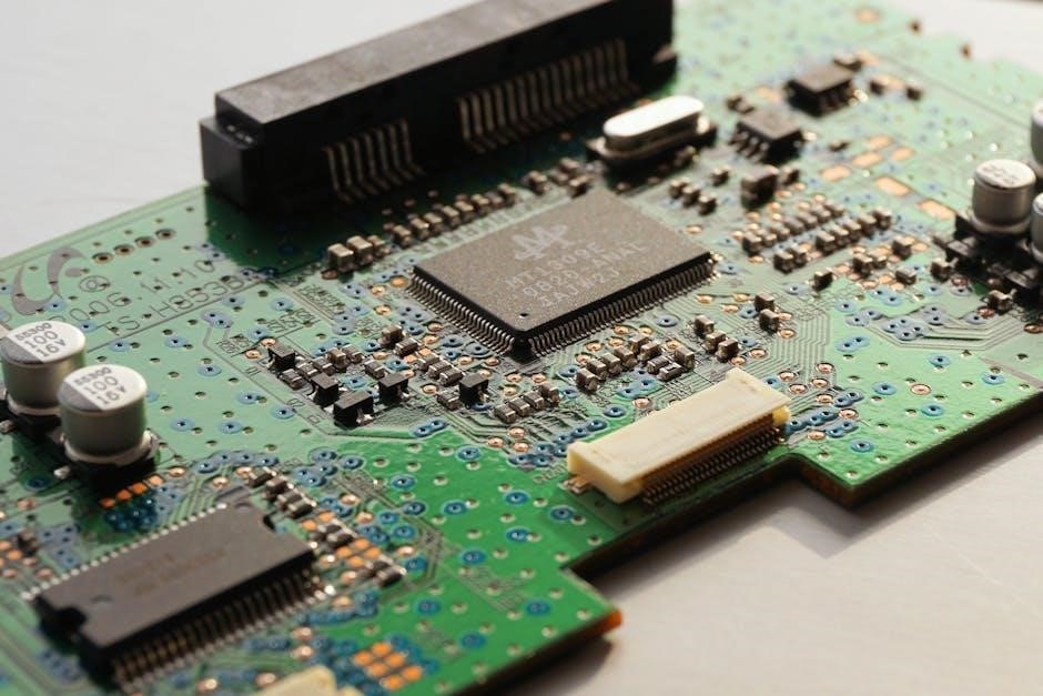
A printed circuit board (PCB) consists of multiple layers, including a substrate (typically fiberglass or plastic), copper circuits, and a solder mask. The substrate provides structural support, while the copper layers enable electrical connections. The solder mask, a protective layer, prevents oxidation and short circuits. Modern PCBs often feature multiple layers stacked together to accommodate complex designs. Additionally, a silkscreen layer is used to label components and reference designators for easy identification. This layered structure ensures reliable connectivity, durability, and efficient performance of electronic components mounted on the board.
Role of the Solder Mask
The solder mask is a protective layer applied to the PCB to prevent oxidation and dust accumulation on the copper circuits. It is typically a liquid photo-imageable lacquer that shields the copper traces, ensuring reliable electrical connections. The solder mask also aids in preventing short circuits by insulating the copper from unintended contacts. Commonly green in color, it provides a visual contrast to help identify components and reference designators. Additionally, the solder mask enhances the durability of the PCB by safeguarding it against environmental factors. This layer is crucial for maintaining the integrity and longevity of the circuit board, especially in harsh operating conditions.
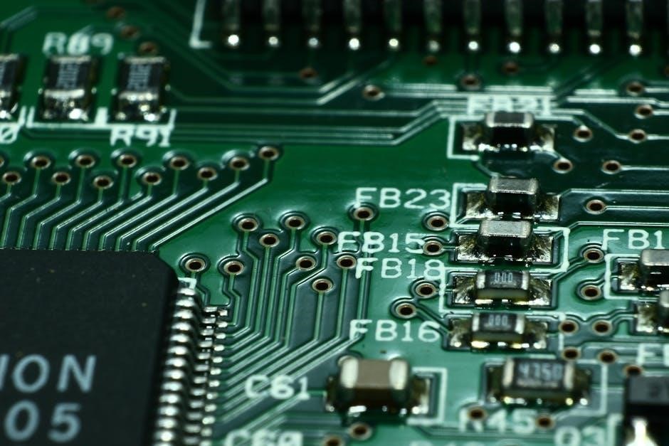
Reference Designators on PCBs
Reference designators are alphanumeric codes assigned to components on a PCB to identify their specific roles. For example, “R1” denotes a resistor, while “C3” indicates a capacitor. These designators are typically printed on the solder mask layer near the component pads, ensuring clear visibility. They guide assembly processes, helping technicians locate and verify components during manufacturing or repair. Reference designators are essential for maintaining organization and accuracy in PCB design, as they standardize component identification across the board. This systematic approach reduces errors and enhances efficiency in both production and troubleshooting, making it a fundamental aspect of circuit board design and functionality.
Methods for Identifying Components
Component identification uses visual inspection, datasheets, and automated tools like AI and machine learning for accurate PCB analysis, ensuring efficient and reliable component recognition and verification.
Visual Inspection Techniques
Visual inspection is a fundamental method for identifying circuit board components. It involves examining the physical attributes of components, such as shape, color, and labeling. The solder mask, a protective green layer, helps prevent oxidation and provides contrast for easier visual recognition. Reference designators, alphanumeric codes on the PCB, guide technicians to specific components. However, visual inspection can be challenging for surface-mount devices (SMDs) due to their small size and lack of clear markings. Magnification tools, such as microscopes or loupe lenses, are often used to enhance accuracy. Proper lighting conditions are essential to avoid glare and ensure clear visibility of component details.
Using Datasheets for Component Recognition
Datasheets are crucial for accurate component recognition, providing detailed specifications and identifiers. They include part numbers, package types, and pin configurations, aiding in verifying component functionality. Cross-referencing with manufacturer databases ensures authenticity and compatibility. Images and diagrams in datasheets help identify physical characteristics, such as SMD markings or through-hole pin layouts. Technical parameters like voltage ratings and capacitance values are also specified, enabling proper component selection. Regularly updated datasheets reflect the latest revisions, ensuring reliability in PCB design and troubleshooting. By leveraging this documentation, engineers and technicians can efficiently identify and validate components, minimizing errors in circuit board assembly and maintenance.
Tools and Software for Automated Identification
Advanced tools and software simplify component identification, enhancing accuracy and efficiency. AI-driven platforms use machine learning algorithms to analyze PCB images, recognizing patterns and components swiftly. Specialized software, like Cadence or Altium, integrates with PCB designs, enabling real-time component tracking. Automated optical inspection (AOI) systems scan boards to detect anomalies and identify components. These tools optimize PCB design, assembly, and quality control, reducing human error. Interactive applications leverage AI for optimizing component placement, while databases and libraries provide reference data. Such solutions streamline workflows, ensuring precise identification and traceability, and are essential for modern electronics manufacturing and maintenance.
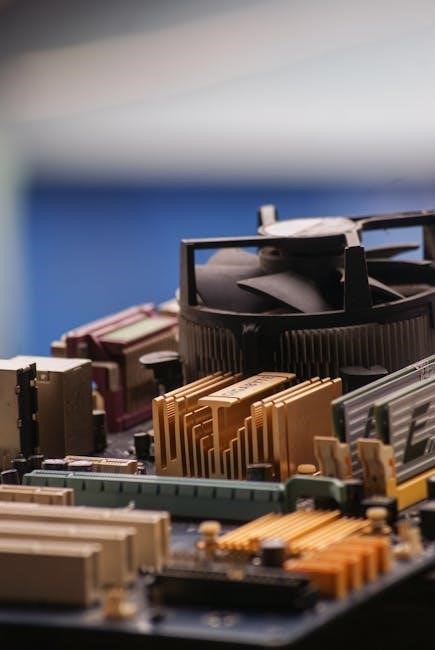
Classification of Circuit Board Components
Circuit board components are classified into through-hole and surface-mount types, with further distinctions between passive and active components, each serving unique roles in PCB design and functionality.
Through-Hole Components
Through-hole components are mounted by inserting leads into PCB holes and soldering them in place. This method provides strong mechanical connection, suitable for high-stress applications. Components like resistors, capacitors, and ICs often use through-hole mounting, though it occupies more space compared to surface-mount technology. The process involves bending leads, inserting them into drilled holes, and soldering on the underside. This traditional method is less common in modern compact devices but remains reliable for durability and ease of repair. Through-hole components are identifiable by their protruding leads and are commonly used in prototyping and high-reliability circuits.
Surface-Mount Devices (SMDs)
Surface-Mount Devices (SMDs) are compact components mounted directly onto a PCB’s surface without through-hole leads. They offer space efficiency and high-density assembly, crucial for modern electronics. SMDs like resistors, capacitors, and ICs have small footprints, enabling miniaturization. Their solder pads are on the component body, requiring precise placement and reflow soldering. SMDs dominate in portable electronics and high-speed applications due to their reduced size, lower weight, and improved signal integrity. Identifying SMDs often relies on part markings or datasheets, as their small size can make visual recognition challenging. Proper handling and automated assembly tools are essential to ensure reliability and performance in SMD-based circuits.
Passive vs. Active Components
Passive components, such as resistors, capacitors, and inductors, operate without an external power source, relying solely on the circuit’s energy. They neither amplify nor switch signals, simply regulating or storing energy. Active components, like transistors and ICs, require a power source to function, enabling signal amplification or switching. Diodes, while not amplifying, control current flow direction, also classified as active. Understanding this distinction aids in PCB troubleshooting and design, as passive components are simpler while active ones perform complex tasks. This classification is essential for identifying and utilizing components effectively in electronic circuits, ensuring proper functionality and efficiency.

Advanced Topics in Component Identification
Advanced methods include AI-driven PCB analysis, optimizing component placement, and automated traceability solutions, enhancing accuracy and efficiency in identifying and managing circuit board components effectively.
AI and Machine Learning in PCB Analysis
AI and machine learning are revolutionizing PCB analysis by enabling automated component recognition and defect detection. These technologies use pattern recognition to identify components and flaws like broken traces or missing parts. Advanced algorithms improve accuracy and efficiency, reducing human error. Machine learning models are trained on datasets of PCB images to enhance identification capabilities. AI-driven tools also optimize component placement, ensuring optimal performance and reducing manufacturing defects. Predictive maintenance is another application, where AI predicts component failures before they occur. This integration of AI and ML in PCB analysis is transforming the electronics industry, making it smarter and more efficient. The future holds even greater potential for innovation in this field.
Optimizing Component Placement
Optimizing component placement on PCBs is crucial for performance, reliability, and thermal management. Proper placement minimizes signal interference and ensures efficient heat dissipation. Advanced software tools use algorithms to analyze component interactions and suggest optimal layouts. This reduces electromagnetic interference and improves signal integrity. Thermal analysis tools identify hotspots, ensuring components are placed to avoid overheating. Automated traceability solutions further enhance placement accuracy, enabling smart manufacturing data generation. By leveraging these technologies, manufacturers can achieve compact, high-performance designs with reduced defects. Effective component placement is vital for meeting functional and reliability requirements in modern electronics. This ensures devices operate efficiently under various conditions.
Automated Traceability Solutions
Automated traceability solutions enhance production by tracking components and ensuring compliance with design specifications. These systems use advanced algorithms to identify and document parts on PCBs, improving quality control. By integrating with manufacturing software, they generate detailed reports for compliance and analysis. This ensures accurate component placement and reduces defects, optimizing production efficiency. Automated solutions also enable real-time monitoring, reducing errors and improving operational transparency. Their ability to handle complex PCBs makes them essential for modern electronics manufacturing, ensuring reliable and consistent outcomes. This technology is pivotal in streamlining processes and meeting industry standards, driving innovation in PCB production.
Common Components Found on Circuit Boards
Resistors, capacitors, ICs, diodes, and transistors are frequently found on PCBs. These components regulate voltage, store energy, and amplify signals, forming the backbone of electronic circuits.
Resistors and Capacitors
Resistors and capacitors are fundamental circuit board components. Resistors regulate voltage and current, identified by color-coded bands or surface-mount labels. Capacitors store electrical energy, with values marked on their bodies. They come in various types, such as ceramic, electrolytic, and film capacitors, each suited for specific applications. Both components are essential for filtering, timing, and voltage regulation in electronic circuits. Their proper identification ensures accurate PCB functionality and performance. Visual inspection and datasheets are key tools for recognizing these components. Understanding their roles and ratings is crucial for circuit design and troubleshooting. Proper placement and selection prevent overheating and ensure reliable operation.
Integrated Circuits (ICs)
Integrated Circuits (ICs) are complex circuit board components containing multiple electronic circuits on a single chip of semiconductor material. They are identified by their unique part numbers and packages, such as DIP, SOIC, or BGA. ICs perform a wide range of functions, from logic operations to signal processing. Their identification is critical for PCB functionality, as they often serve as the brain of the circuit. Visual inspection, datasheets, and automated tools are essential for recognizing ICs. Proper handling and soldering techniques prevent damage. ICs are categorized into analog, digital, or mixed-signal types, each requiring specific placement and testing for optimal performance.
Diodes and Transistors
Diodes and transistors are fundamental circuit board components. Diodes, typically marked with a stripe indicating the cathode, allow unidirectional current flow. Transistors, with three terminals (collector, base, emitter), act as switches or amplifiers. On PCBs, diodes are often labeled with “D” and transistors with “Q.” Visual inspection and schematic matching help identify them. Using a multimeter, diodes can be tested for forward/reverse voltage, while transistors are tested for junction integrity. Datasheets provide specifications, aiding identification. Diodes may be near power sources, and transistors in switching sections. Practice and online guides enhance identification skills, combining visual, schematic, and electrical testing methods for accuracy.
Quality Control and Inspection
Quality control ensures PCB components are accurately identified and placed, using reference designators and automated traceability solutions to maintain reliability and functionality.
Identifying Defects on PCBs
Identifying defects on PCBs involves detecting issues like soldering faults, missing components, or broken traces. Automated solutions and AI-driven tools enhance defect recognition accuracy. Regular inspections ensure early detection of anomalies, preventing functional failures and ensuring reliability. Proper component placement and solder mask integrity are critical to avoid common defects. Advanced algorithms can analyze PCBs for inconsistencies, such as improper alignment or oxidation. High-quality images and detailed datasheets aid in identifying flaws. Accurate defect detection is essential for maintaining PCB performance and longevity.
Importance of Component Placement Accuracy
Accurate component placement is crucial for ensuring proper PCB functionality. Misaligned or improperly placed components can lead to electrical failures, reduced performance, and reliability issues. Advanced algorithms and AI-driven tools optimize placement, minimizing errors. Solder mask protection prevents oxidation and dust contamination, ensuring components remain functional. Precise placement is especially critical for through-hole and surface-mount technologies, where even minor misalignments can cause defects. Automated traceability solutions enhance placement accuracy, generating smart manufacturing data. This ensures components are correctly positioned, maintaining the integrity of the circuit board and preventing operational failures. Proper placement is key to achieving high-quality PCBs.
Resources for Component Identification
Resources for component identification include online databases, stock images, and interactive tools. These aids help in recognizing and understanding circuit board components effectively.
Online Databases and Libraries
Online databases like Digi-Key and Mouser provide extensive libraries of component specifications. These resources enable quick identification and verification of parts on circuit boards, ensuring accuracy and efficiency in design and repair.
Stock Images and Vector Graphics
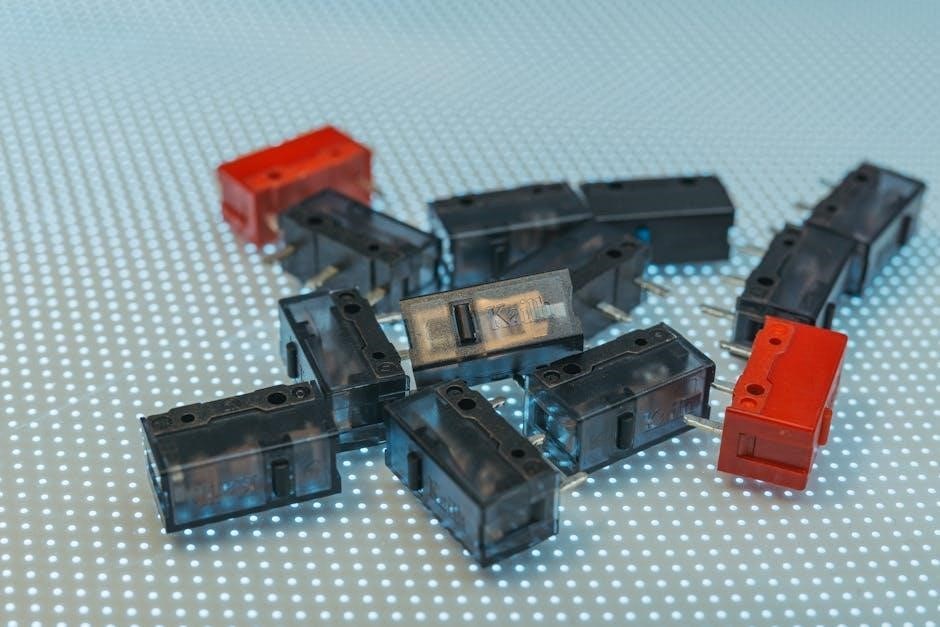
Stock images and vector graphics are invaluable for visually identifying circuit board components. Websites like iStock and Getty Images offer high-quality images of components such as resistors, capacitors, and ICs. These visuals aid in recognizing parts by their shape, size, and packaging, making identification easier for both professionals and hobbyists. Detailed illustrations can highlight specific features, such as terminal layouts or SMD markings, which are crucial for accurate component recognition. These resources are particularly useful for educational purposes, DIY projects, and quality control processes. By referencing these images, individuals can cross-verify components, ensuring correct identification and proper functionality in their designs or repairs. Many platforms provide these images for download, supporting technical documentation and creative projects alike.
Interactive Applications for PCB Analysis
Interactive applications for PCB analysis are revolutionizing component identification by leveraging AI and machine learning. These tools enable users to optimize component placement and detect flaws like broken traces or improper positioning. Advanced apps utilize real-time scanning and databases to recognize components, enhancing accuracy and efficiency. They also support automated traceability, generating data for smart manufacturing. Such applications are invaluable for education, design, and troubleshooting, providing interactive visuals and detailed insights. By integrating AI-driven algorithms, these platforms offer innovative solutions for PCB analysis, making complex tasks more accessible and streamlining the identification process.
Understanding circuit board components is crucial for ensuring functionality and quality. Advances in AI and machine learning promise enhanced identification and analysis for future PCB design and manufacturing.
Future Trends in Component Identification
Emerging technologies like AI and machine learning are revolutionizing component identification, offering enhanced accuracy and speed. Augmented reality tools are being integrated for immersive PCB analysis and training. Advances in 3D scanning and X-ray imaging enable deeper inspection of hidden components. Predictive maintenance, leveraging data analytics, will foresee potential failures, reducing downtime. Additionally, automated traceability solutions are expected to streamline smart manufacturing processes. These innovations promise to make component identification faster, more precise, and scalable for complex PCB designs, driving efficiency in electronics production and ensuring higher quality standards.
Best Practices for PCB Component Recognition
Effective PCB component recognition involves understanding reference designators, using datasheets for accurate identification, and employing visual inspection techniques. Prioritize high-quality images and diagrams to avoid ambiguities. Utilize tools like solder mask inspection to identify protective layers and prevent oxidation. Leverage interactive applications for immersive PCB analysis and training. Stay updated with advancements in AI and machine learning for enhanced recognition accuracy. Regularly cross-reference components with reliable databases and libraries to ensure correctness. Implementing these best practices ensures efficient and precise component identification, minimizing errors and improving overall PCB functionality and reliability in electronics manufacturing and repair processes.